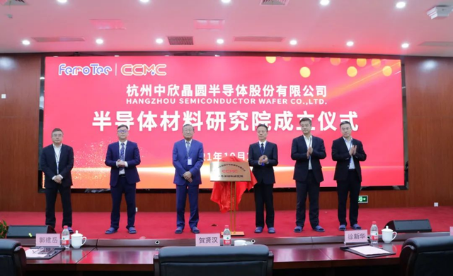

On October 28, the semiconductor materials research institute of Hangzhou Zhongxin wafer semiconductor Co., Ltd. (hereinafter referred to as "semiconductor materials research institute") held the Establishment Ceremony.
Zhongxin wafer news shows that the semiconductor materials research institute is built by Zhongxin wafer and plans to cooperate with universities and laboratories to focus on the research and development of semiconductor silicon material technology and testing analysis.

It is reported that the headquarters of semiconductor materials research institute is set up in Zhongxin wafer Hangzhou headquarters. The main research directions of the Institute are the application-oriented physical and chemical research of light doped and heavy doped silicon single crystals, the development of single crystal forming technology, the development of silicon wafer (epitaxial wafer) processing technology, and the development and application of detection and analysis technology. The team members are mainly doctors and masters, and hire relevant professionals from relevant universities and research institutes to participate. The participants have many years of R & D experience in the semiconductor industry and participate in various types of semiconductor silicon wafer projects. The R & D technical team will serve the research, development and application of crystal forming, silicon wafer (epitaxial wafer) processing technology and monitoring and analysis technology related to semiconductor silicon single crystal. The Institute is a new R & D institution that is market-oriented, combines industry, University and research, develops single crystal and silicon wafer processing, testing and analysis technologies, and seamlessly connects with the market.
It is reported that Zhongxin wafer is a "versatile and chain leading enterprise" in the field of silicon wafer production in China. Its products cover a full range of 6 inches and below, 8 inches and 12 inches. The polished and epitaxial chips produced are mainly used in core fields such as logic chips, flash memory chips, dynamic random memory chips, image sensors and display driver chips, In particular, the manufacturing field of 12 inch epitaxial wafer has reached the international advanced level.