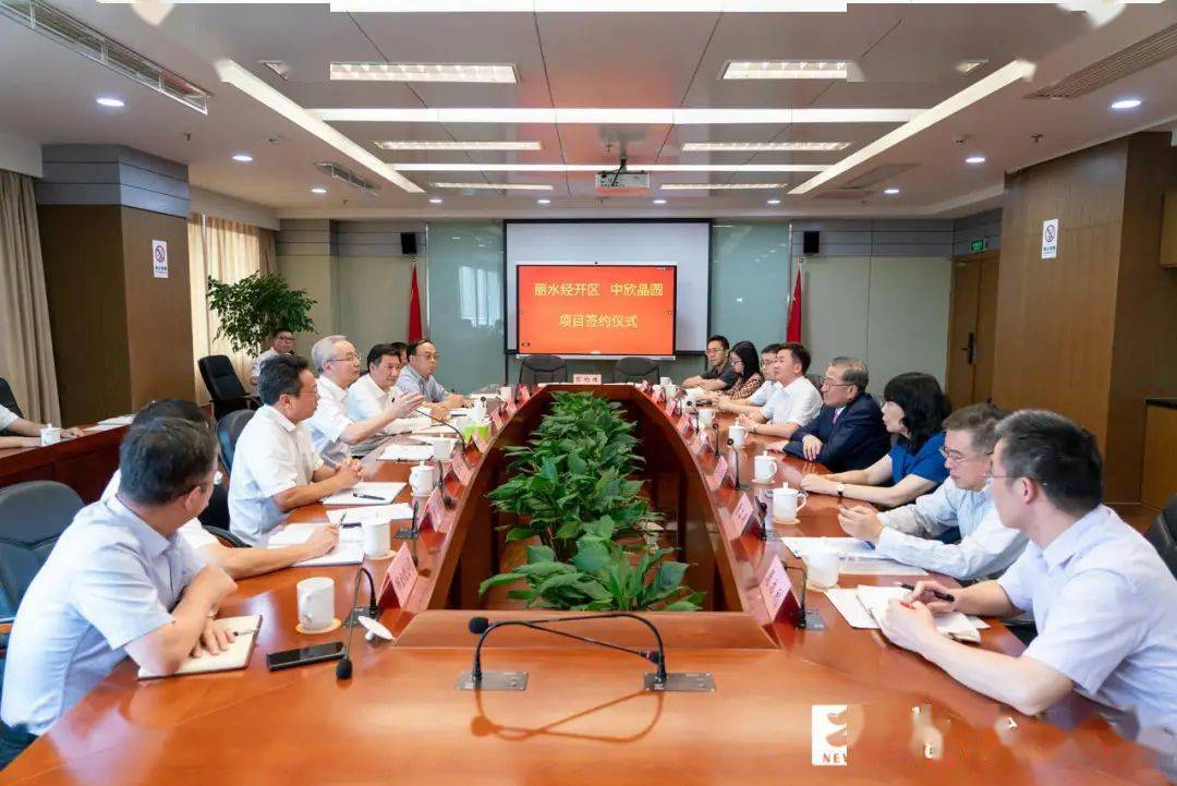

Recently, Hangzhou Semiconductor Wafer Co.,Ltd., the domestic leader in high-end chip wafer production, held a project signing ceremony with Lishui Economic and Technological Development Zone to build the "8-inch (200mm) and 12 inch (300mm) epitaxial wafer project", with a total investment of 4 billion yuan. After all, the annual output value will reach about 5 billion yuan.

According to the person in charge of Zhongxin wafer, the current design capacity of Lishui Zhongxin project is 100000 pieces of 8 inches and 200000 pieces of 12 inches per month. In the future, we will expand the capacity according to market changes and strive to build Lishui into an "extension capital".
In recent years, Lishui has taken the cultivation of the whole semiconductor chain industry as an important strategic measure in building a modern ecosystem, laid out and built a "thousand mu chip industrial park", and accurately introduced chip design, materials, manufacturing, packaging, testing, equipment, application and other industrial chain projects with the third-generation power semiconductor and optoelectronic frontier as the main direction.
According to the introduction of "Lishui Economic Development Zone", at present, Lishui has landed 11 projects such as semiconductor Research Institute of Chinese Academy of Sciences, Jiangfeng electronics, Jingrui electronics, Juexin microelectronics and Yixin semiconductor, with a total investment of 17.9 billion yuan, and has successively contacted and connected with "leading enterprises, chain leading enterprises and benchmark enterprises" in domestic semiconductor industries such as Zhongxin wafer, Shilan micro, Leon micro and Zhengfan technology, Promote the implementation of the project.
At present, the demand for 8-inch and 12 inch large silicon wafers is blowout, but it mainly depends on imports, and the supply of 12 inch large silicon wafers will continue to be in short supply for several years. As one of the largest semiconductor wafer manufacturers in China, Zhongxin wafer is also the first enterprise in China that can independently complete the R & D and production from 12 inch single crystal and polishing to epitaxy. With the landing of Zhongxin project in Lishui, it also marks that Lishui has joined a "global 12 inch semiconductor wafer card battle".
Chen Lei, deputy director of the management committee in charge of investment promotion of Lishui Economic Development Zone, said that Lishui Economic Development Zone has initially formed the industrial prototype of the whole semiconductor chain. With the completion and production of Zhongxin wafer, Jingrui electronics and other projects, Lishui will become one of the main production areas of large-size epitaxial wafers in China, and build a national epitaxial wafer production, R & D and manufacturing base in the future.